Getting Started with FPGAs

Reconfigurable Hardware
A chip you configure yourself. No prior electronics needed — start here, and by the end you'll know what an FPGA is, what's inside one, how designs are described, and what tools you need to build your first one.
Understanding FPGAs
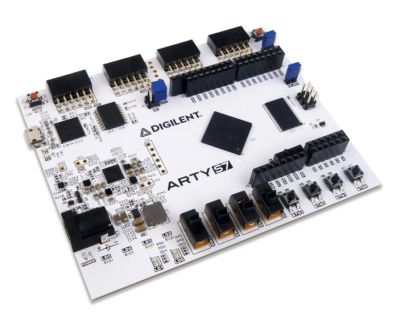
Field-Programmable Gate Array
FPGA stands for Field-Programmable Gate Array. The name tells you most of what you need to know: it's an array of digital logic you can program out in the field — after the chip has been manufactured, on your own desk, as many times as you like.
That makes it different from the two things around it. A microcontroller like the Raspberry Pi Pico has fixed hardware and runs your software one instruction at a time. An ASIC is custom silicon, fast and cheap in volume, but the design is frozen at the factory. An FPGA sits in between: you describe actual circuits, and the chip rearranges itself to become them. Change your mind, reload the chip, and it's different hardware a second later.
The payoff is parallelism. Because you're building real circuits rather than queuing instructions, hundreds of things can happen on the same clock edge — which is why FPGAs show up in video processing, radar, high-speed networking, test equipment, and anywhere microsecond-scale latency matters. And because they're reprogrammable, they follow the same design flow as custom silicon without the enormous one-time cost of building a chip.
Three Ways to Build Digital Logic
Microprocessors/Microcontrollers
Fixed hardware, flexible software. Cheap, simple, sequential.
FPGA
Hardware you define and redefine. Parallel, fast, reprogrammable.
ASIC
Custom silicon. Fastest and cheapest at volume — but frozen forever.
FPGA Architecture
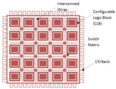
Open up an FPGA and you find a regular grid — a sea of small logic tiles, with programmable wires running between them. The tiles are called Configurable Logic Blocks (CLBs), and each one holds a handful of lookup tables, flip-flops, multiplexers, and fast carry logic. In AMD 7 Series parts, a CLB contains two slices, and a slice holds four 6-input lookup tables plus eight flip-flops. That's the whole trick: a lookup table stores a truth table in tiny memory, so it can become any logic function of its inputs, and a flip-flop remembers one bit between clock edges.
Logic alone isn't enough, so modern FPGAs mix in dedicated hardware. Columns of block RAM give you real on-chip memory instead of burning thousands of flip-flops. DSP slices are hardwired multiply-accumulate units that do in one clock cycle what would otherwise consume hundreds of lookup tables. I/O blocks around the edge drive the physical pins at whatever voltage standard your board needs, and high-speed transceivers handle serial links. Some devices go further and put a full processor on the same die — AMD's Zynq family pairs Arm cores with FPGA fabric, which is what the Arty Z7 board above is built around.
Knowing this layout changes how you design. When the tools report your usage in LUTs, flip-flops, BRAM, and DSP, they're telling you how much of each physical resource you consumed — and good designers steer work toward the right one on purpose.
FPGA Resources
Look-Up Table:LUT
A tiny memory holding a truth table. A 6-input LUT can implement any Boolean function of 6 inputs.
Flip-Flop: FF
Stores one bit, updated on a clock edge. The basis of all sequential logic and pipelining.
Configurable Logic Block: CLB
The repeating tile of the fabric — LUTs, flip-flops, muxes and carry logic grouped into slices.
Block RAM: BRAM
Dedicated on-chip memory blocks, usable as RAM, ROM or FIFOs — far cheaper than flip-flops.
DSP Slice: DSP
Hardwired multiplier and accumulator. Essential for filters, math and signal processing.
Input/Output Block: IOB
The interface to real pins — programmable buffers supporting different voltage standards.
FPGA Development Environment

FPGA Tools
Getting from HDL to a working chip is an automated pipeline, and it's worth knowing the stages by name. Synthesis translates your code into a netlist of real primitives — LUTs, flip-flops, DSP blocks. Implementation then places those primitives into specific CLBs on the die and routes the programmable interconnect to connect them, trying to keep the longest signal path short enough to meet your clock speed. Finally, the tools generate a bitstream: a binary file encoding the state of every programmable element and routing switch. Load it over USB/JTAG and the chip becomes your design.
Each vendor ships one big tool that does all of this. For AMD parts it's the Vivado Design Suite, and the important news for a beginner is that Vivado ML Standard Edition is free and requires no license — it covers Spartan-7, Artix-7, and selected Zynq-7000 and Kintex-7 devices, which is exactly the range of affordable hobbyist boards. Altera users run Quartus Prime, Lattice users Radiant or Diamond, and Microchip users Libero; all have free tiers. There's a good open-source path too: Icarus Verilog or Verilator with the GTKWave viewer let you write and simulate HDL on any computer before you own a board at all.
For hardware, pick an inexpensive board with an on-board programmer and good documentation, and don't start with a large design. Get an LED blinking from a counter, then a switch-driven state machine, then something that talks to a PC. Every project on this site started that way.
Step 1: Write and Simulate
HDL plus a testbench. Check the waveforms before anything else.
Step 2: Synthesize
Code becomes a netlist of LUTs, flip-flops and dedicated blocks.
Step 3: Place & Route
Primitives land in real CLBs; interconnect is routed to meet timing.
Step 4: Configure the FPGA
A bitstream loads over JTAG or SPI — and the chip is your circuit.
Hardware Description Language (HDL)
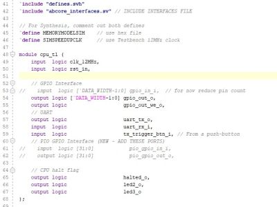
Verilog/SystemVerilog HDL
You don't draw an FPGA design gate by gate. You describe it, in a Hardware Description Language — most often Verilog, its modern superset SystemVerilog, or VHDL. It looks a little like C, and that resemblance is the single biggest trap for beginners: HDL code is not a list of steps to execute. It is a description of hardware that all exists at once. Every line you write becomes wires and gates that are permanently there, doing their job on every clock edge.
Designs are written at the register-transfer level (RTL): you say which registers hold what, and what combinational logic sits between them. You build in modules — a counter, a shift register, a state machine — then wire modules together into bigger ones, the same way you'd assemble subsystems on a schematic. Verilog and SystemVerilog dominate in the US industry; VHDL is more common in Europe and aerospace. Either is a fine place to start, and the ideas transfer.
Before anything touches hardware you simulate. You write a testbench that feeds your module inputs and checks its outputs, and you watch the waveforms. Simulation is where most of an FPGA engineer's time goes, and it is the habit that separates designs that work from designs that mysteriously don't.